
Introduction
What if you could create a functional combination lock without a single line of code? No microcontroller, no logic ICs, just transistors, resistors, capacitors, switches, and LEDs (indicator detecting change of state).
Welcome to the fascinating world of transistor-based combination locks, a brilliant demonstration of how basic electronic components can be orchestrated into a secure and functional sequential logic circuit. This circuit behaves like a memory chain: it only allows current to flow through a final load (for demonstration purposes we used an LED) if a specific sequence of switches is activated correctly. The mechanism behind it is a clever interplay of NPN bipolar junction transistors (BJTs), RC timing elements, and discrete state memory, all wired into a cascading structure.
In this article, we will explore how this system works, building our understanding from the ground up and diving into the role of each component. By the end, you'll not only appreciate the elegance of discrete design, but you'll also gain practical insight into transistor switching, biasing, capacitive coupling, and sequential logic.
System Overview
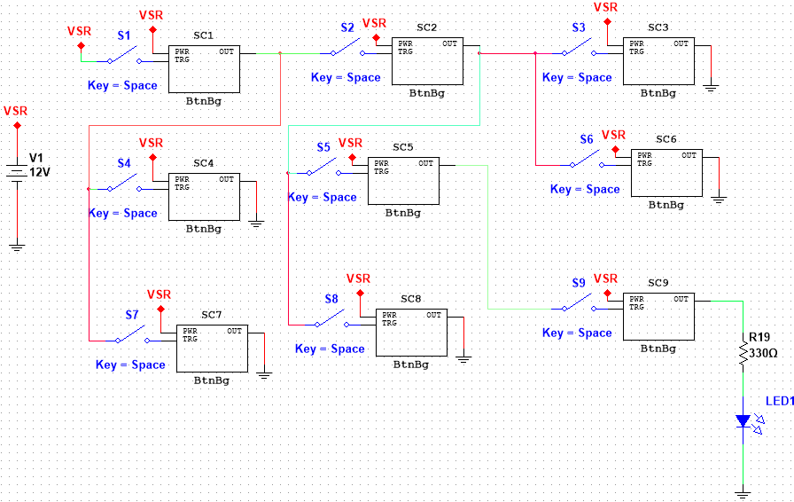
Complete Keypad Circuit
Correct Key Chain Circuit
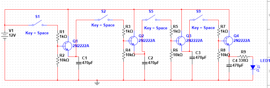
The transistor-based combination lock you see above is composed of:
- 4 NPN Transistors (Q1-Q4), acting as sequential gates.
- 4 Momentary Pushbutton Switches (S1-S9), used to input the correct combination.
- Electrolytic Capacitors (6.8µF/50V (in this case)), used for pulse storage and signal coupling.
- Resistors, for current limiting, pull-down biasing, and LED control.
- 1 LED, as the final output indicator of a correct sequence.
The combination lock works by creating a chain of interdependent transistor switches. Each transistor stage must be enabled by the correct prior condition, meaning the corresponding switch must be pressed only after the previous switch in the sequence. Pressing the wrong button resets the chain, preventing accidental unlocking.
Let’s now dig deep into each stage, starting with Switch 1 (S1) and Transistor Q1.
Stage 1: S1 and Q1, The First Gate
Wiring and Function:
- S1 Terminal 1 connects to VCC (positive supply).
- S1 Terminal 2 connects to the base of Q1 through a 1kΩ resistor.
- The base of Q1 is also connected to GND through a 10kΩ pull-down resistor.
- The emitter of Q1 connects to GND via a 6.8µF/50V electrolytic capacitor.
- The collector of Q1 connects to VCC through a 1kΩ resistor.
Operation:
- This is a classic switching stage for an NPN transistor. The idea is to turn Q1 on momentarily when S1 is pressed.
- When S1 is not pressed, the 10kΩ pull-down keeps the base of Q1 at 0V, and Q1 remains off.
- When S1 is pressed, a voltage is applied to the base of Q1 through the 1kΩ resistor.
- This forward-biases the base-emitter junction, turning on Q1.
- The capacitor at the emitter provides a kind of pulse memory, it charges during this moment and maintains a small residual voltage for a short time.
- The collector of Q1, pulled high through 1kΩ, will pull low during conduction, allowing current to flow and signal the next stage.
The clever part is that this stage doesn’t just pass a signal forward, it only enables the next stage briefly. Once the emitter capacitor discharges, Q1 turns off again.
Stage 2: S2 and Q2, Sequential Enforcement
Connections:
- One terminal of S2 connects to the emitter of Q1.
- The other terminal of S2 connects to the base of Q2 via a 1kΩ resistor.
- The base of Q2 is pulled down with a 10kΩ resistor to GND.
- The emitter of Q2 connects to GND via a 6.8µF capacitor.
- The collector of Q2 connects to VCC via a 1kΩ resistor.
Operation:
- Now the magic begins: S2 will only activate Q2 if the emitter of Q1 is high, which only happens after S1 has been pressed.
- When S1 is pressed, the capacitor at Q1’s emitter charges.
- If S2 is pressed while Q1's emitter is still charged, the base of Q2 sees a voltage, turning it on.
Just like in Q1’s stage, turning on Q2 causes its collector to go low, preparing the input condition for stage 3.
This condition enforces sequence:
- If you press S2 before S1, Q1’s emitter is at 0V, and pressing S2 does nothing.
- If you press S2 after S1, within a short time window (before the cap discharges), Q2 activates.
- This is time-sequenced logic without a microcontroller, pure analog engineering.
Stage 3 and Stage 4: (S5, Q3) and (S9 , Q4)
These two stages are exact replicas of Stage 2, creating an extended combination sequence.
Functional Implications:
- Each stage depends on the charge held by the capacitor at the previous stage’s emitter. These small capacitors hold enough charge for a few seconds, giving a short time window to press the next switch.
- If you press a switch too early or too late, the corresponding transistor base gets no voltage, and the sequence breaks.
This way, only the correct timing and sequence of S1 → S2 → S5 → S9 will allow the chain to propagate.
Final Output: LED Activation
- Once Q4 is activated, we reach the final stage of the lock:
- The emitter of Q4 (now active) connects through a 330Ω resistor to the anode of an LED.
- The cathode of the LED is grounded.
How It Works:
- When Q4 is properly activated by pressing S9 in sequence, the emitter becomes a voltage source.
- The LED receives current through the 330Ω resistor, limiting it to safe operating levels (around 10-15mA).
The LED lights up, signaling a successful code entry.
If the sequence is broken at any point, Q4 never turns on, and the LED stays dark.
System Behavior Summary:
Step Condition Result
-
S1 Pressed → Base of Q1 triggered Q1 turns on briefly
-
S2 Pressed during Q1 emission Q2 turns on
-
S5 Pressed during Q2 emission Q3 turns on
-
S9 Pressed during Q3 emission Q4 turns on
-
Q4 On → Emitter powers LED LED lights up
-
If any switch is pressed out of sequence, or too slowly, the prior transistor does not supply voltage to the next base, and the chain breaks.
Potential Improvements and Customizations
Longer sequences: Add more stages with additional Qn and Sn pairs.
Additional Resources
Keep Reading
Related Articles
Comments
Sign in to join the discussion.
Loading comments…